
By v | 29 September 2026 | 0 Comments
What Does "Near-Net-Shape" Really Mean for Reaction-Bonded Silicon Carbide?
1. Introduction: Why Near-Net-Shape Matters in Advanced Ceramics
1.1 What Is Near-Net-Shape?
Near-net-shape is a manufacturing term that describes a process where the final product is formed very close to its desired dimensions. In conventional ceramic manufacturing, the sintering process often causes significant shrinkage — sometimes as much as 15–20% — which means the green body must be made oversized to compensate. This shrinkage is unpredictable and can vary from batch to batch, making it difficult to achieve tight tolerances without extensive machining.Near-net-shape manufacturing minimizes this shrinkage, allowing the final product to match the mold dimensions more closely. For Reaction-Bonded Silicon Carbide (SiSiC) , the sintering shrinkage is less than 1%, which is exceptionally low for a ceramic material. This near-net-shape capability is one of the most important advantages of Reaction-Bonded Silicon Carbide (SiSiC) and a key reason why it is widely used for complex, dimensionally precise components.
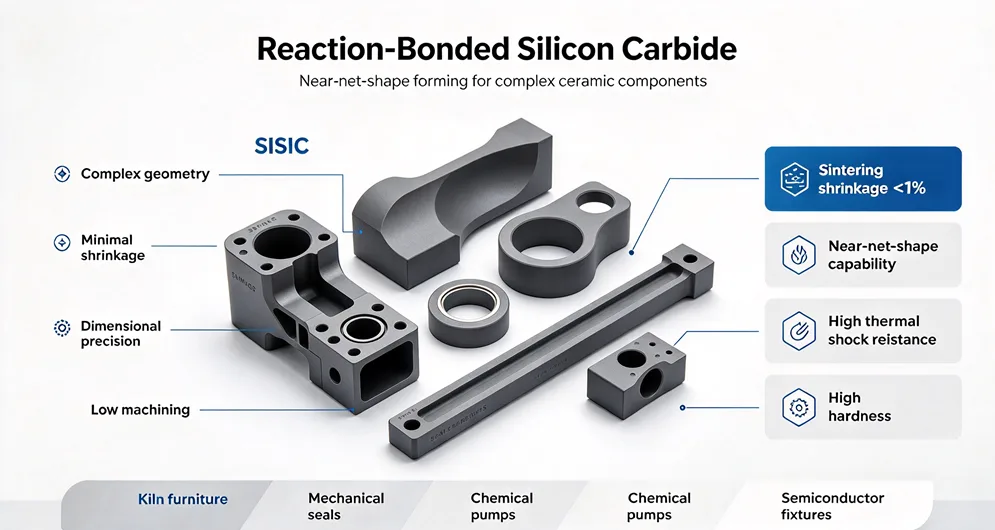
Reaction-Bonded Silicon Carbide
1.2 Why Shrinkage Is a Problem for Ceramics
Ceramics are inherently brittle and difficult to machine. Diamond grinding is the primary method for shaping fired ceramic components, but it is slow, expensive, and limited in the geometries it can produce. Complex features such as internal channels, undercuts, and fine details are difficult or impossible to machine.If a ceramic component shrinks significantly during sintering, the manufacturer must either accept looser tolerances or invest in extensive machining to achieve the required dimensions. Both options increase cost and lead time. Near-net-shape manufacturing reduces or eliminates this problem, allowing complex geometries to be produced with minimal post-processing.
1.3 Why Reaction-Bonded Silicon Carbide (SiSiC) Excels at Near-Net-Shape
Reaction-Bonded Silicon Carbide (SiSiC) is particularly well-suited to near-net-shape manufacturing because of its unique reaction bonding process. Unlike conventional sintering, which relies on solid-state diffusion and causes significant shrinkage, the reaction bonding process uses a chemical reaction between molten silicon and carbon to form new silicon carbide that bonds the structure together. This reaction occurs with minimal dimensional change, allowing the final product to maintain the shape and dimensions of the original preform.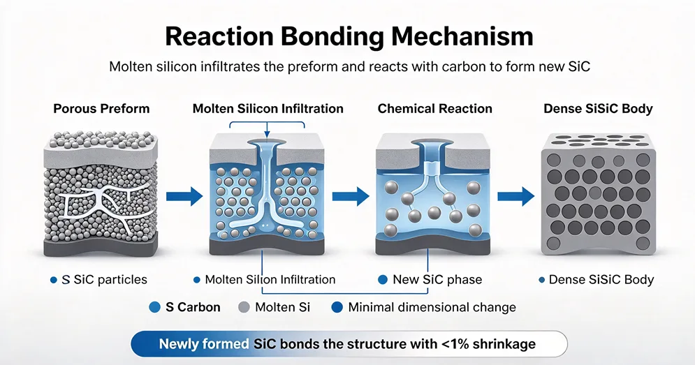
Reaction Bonding Mechanism
2. Understanding Reaction-Bonded Silicon Carbide
2.1 What Is Reaction-Bonded Silicon Carbide (SiSiC) ?
Reaction-Bonded Silicon Carbide (SiSiC) , also known as RB-SiC, is an advanced engineering ceramic manufactured through a unique reaction bonding process. The final product primarily consists of silicon carbide (SiC) and a small amount of remaining free silicon (Si) phase. Its fundamental difference from process routes like pressureless sintering and hot pressing lies in the fact that a chemical reaction occurs during the sintering process, utilizing the newly formed phase from the reaction to densify the material.The typical composition of Reaction-Bonded Silicon Carbide (SiSiC) includes 98.5–99% SiC and 1–1.5% free silicon, depending on the manufacturing process and intended application. The microstructure consists of SiC grains surrounded by a continuous silicon network, with very low porosity (≤0.1%).
2.2 Key Properties of Reaction-Bonded Silicon Carbide (SiSiC)
Reaction-Bonded Silicon Carbide (SiSiC) offers a combination of properties that make it suitable for demanding industrial applications.Near-net-shape forming: Extremely low sintering shrinkage (<1%), enabling the production of complex, dimensionally precise components with minimal post-processing.
Exceptional thermal properties: High thermal conductivity (120 W/m·K at 20°C) and outstanding thermal shock resistance, performing reliably under rapid temperature changes.
Superior hardness and wear resistance: With a Mohs hardness of 13, it is an excellent material for abrasive and wear-intensive environments.
High strength and stiffness: Flexural strength of 250 MPa at 20°C and 280 MPa at 1200°C, with an elastic modulus of 330 GPa.
Good corrosion resistance: Highly resistant to most acids, alkalis, and salt solutions, though vulnerable to hydrofluoric acid and hot, concentrated caustics due to the free silicon content.
2.3 Why Near-Net-Shape Is a Game-Changer
The near-net-shape capability of Reaction-Bonded Silicon Carbide (SiSiC) is a game-changer for ceramic manufacturing. It allows complex geometries to be produced with minimal machining, reducing cost and lead time. It also enables the production of features that would be difficult or impossible to machine, such as internal channels, complex curves, and fine details.For industries that require high-performance ceramic components with complex shapes — such as semiconductor manufacturing, kiln furniture, and wear-resistant components — the near-net-shape capability of Reaction-Bonded Silicon Carbide (SiSiC) is a significant advantage.
3. Why Near-Net-Shape Forming Is Difficult for Ceramics
3.1 The Shrinkage Problem
Most ceramic manufacturing processes involve sintering, where the ceramic powder is heated to a high temperature to densify and strengthen the material. During sintering, the particles bond together and the material shrinks. The amount of shrinkage depends on the material, the particle size, the sintering temperature, and other factors.For many ceramics, the shrinkage can be 15–20% or more. This means that the green body (the unfired ceramic shape) must be made significantly larger than the final product. Predicting and controlling the shrinkage is difficult, and variations in shrinkage can lead to dimensional inaccuracies and rejected parts.
3.2 The Machining Problem
To achieve tight tolerances, fired ceramic components often require diamond grinding. This is a slow and expensive process, and it is limited in the geometries it can produce. Complex features such as internal channels and undercuts are difficult or impossible to machine.The combination of shrinkage and machining requirements makes conventional ceramic manufacturing expensive and time-consuming, particularly for complex components.
3.3 How Reaction-Bonded Silicon Carbide (SiSiC) Solves Both Problems
Reaction-Bonded Silicon Carbide (SiSiC) solves both problems through its unique reaction bonding process. Because the process occurs with minimal shrinkage (<1%), the final product closely matches the mold dimensions. This eliminates the need for oversized green bodies and reduces the need for diamond grinding.The reaction bonding process also allows complex shapes to be produced directly from the preform, without the need for extensive machining. This makes Reaction-Bonded Silicon Carbide (SiSiC) ideal for complex, dimensionally precise components.
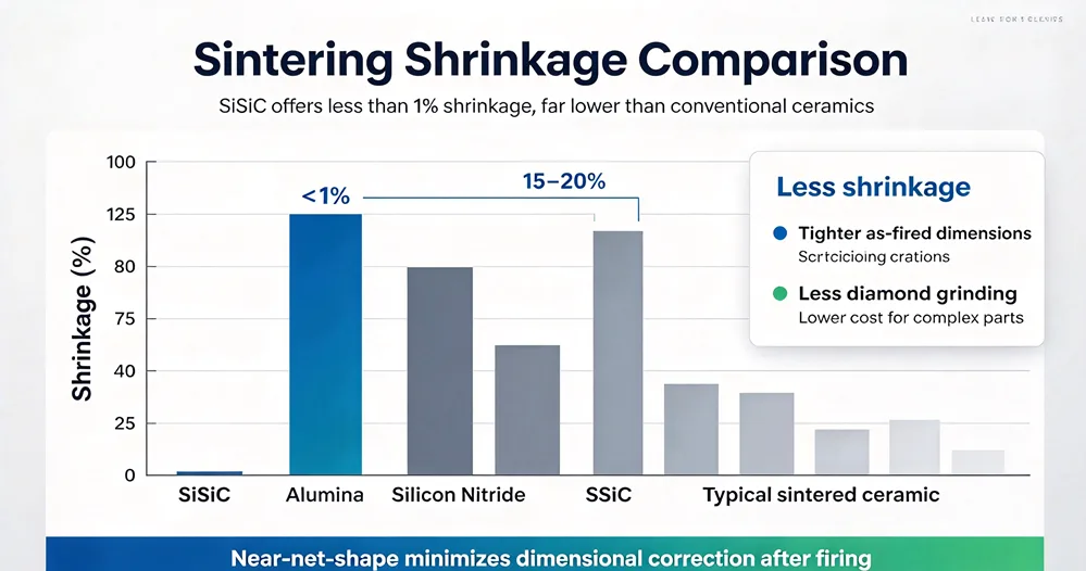
Sintering Shrinkage Comparison
4. How the Reaction Bonding Process Achieves Near-Net-Shape
4.1 Step 1: Preparing the Preform
The reaction bonding process begins with the preparation of a porous preform containing SiC particles and carbon. The preform is shaped using conventional ceramic forming techniques such as slip casting, pressing, or extrusion. The preform has the desired shape of the final product, with allowance for minimal dimensional change during processing.4.2 Step 2: Infiltrating with Molten Silicon
The shaped preform is then heated in a furnace and infiltrated with molten silicon. The molten silicon wicks into the porous preform through capillary action, filling the spaces between the SiC particles and the carbon.4.3 Step 3: Chemical Reaction
The molten silicon reacts with the carbon in the preform to form additional SiC. This reaction is exothermic and occurs rapidly, bonding the original SiC particles together and filling the remaining porosity. The newly formed SiC is deposited on the surfaces of the existing SiC particles, growing them and creating a continuous network.4.4 Step 4: Minimal Dimensional Change
The key to near-net-shape forming is that the reaction bonding process occurs with minimal dimensional change. The silicon infiltrates the preform and reacts with the carbon, but the overall dimensions of the preform are maintained. The shrinkage is typically less than 1%, which is exceptionally low for a ceramic material.4.5 Step 5: Cooling and Finishing
After the reaction is complete, the material is cooled. The result is a dense, strong ceramic body with the desired shape and dimensions. Minimal finishing is required, typically limited to light grinding or polishing to achieve the final surface finish.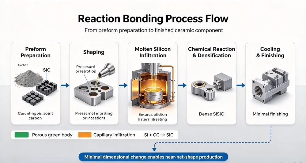
Reaction Bonding Process Flow
5. What Near-Net-Shape Means for Design and Manufacturing
5.1 Design Freedom
Near-net-shape forming gives designers greater freedom to create complex geometries. Features that would be difficult or impossible to machine — such as internal channels, curved surfaces, and fine details — can be produced directly in the mold. This opens up new possibilities for component design and optimization.5.2 Cost Reduction
Near-net-shape forming reduces cost in several ways. It eliminates the need for oversized green bodies, reduces the need for diamond grinding, and minimizes material waste. For complex components, the cost savings can be significant.5.3 Lead Time Reduction
Near-net-shape forming also reduces lead time. Because minimal machining is required, components can be produced faster and delivered sooner. This is particularly important for industries where downtime is costly.5.4 Quality Improvement
Near-net-shape forming improves quality by reducing the risk of machining-induced defects. Diamond grinding can introduce micro-cracks and residual stresses, which can reduce the strength and reliability of the component. By minimizing machining, near-net-shape forming preserves the integrity of the ceramic material.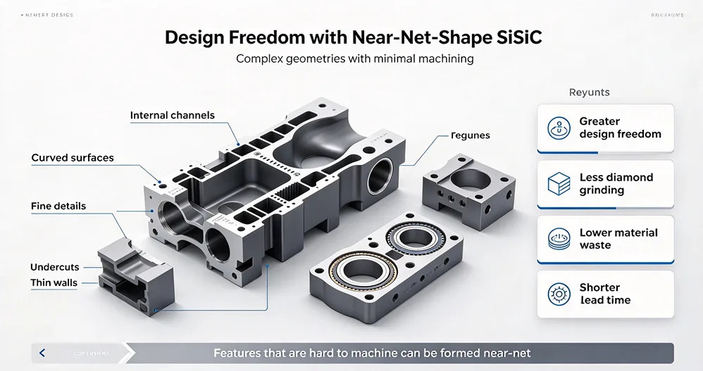
Design Freedom with Near-Net-Shape SiSiC
6. Matching Near-Net-Shape SiSiC to Your Application
6.1 High-Temperature Kiln and Thermal Equipment
The largest application area for Reaction-Bonded Silicon Carbide (SiSiC) is high-temperature kiln and thermal equipment. It is used for rollers, beams, rails, setters, and saggers in furnaces for ceramics, lithium battery materials, and magnetic materials. The near-net-shape capability allows complex kiln furniture shapes to be produced with minimal machining.6.2 Wear and Seal Components
Reaction-Bonded Silicon Carbide (SiSiC) is ideal for mechanical seal rings, wear-resistant liners, and nozzles in mining, power, and pump industries. The high hardness and wear resistance of Reaction-Bonded Silicon Carbide (SiSiC) extend component life, while the near-net-shape capability allows complex seal geometries to be produced.6.3 Chemical Industry
Reaction-Bonded Silicon Carbide (SiSiC) is suitable for pumps and valve components that handle corrosive media with particulate matter. The corrosion resistance of Reaction-Bonded Silicon Carbide (SiSiC) ensures long service life, while the near-net-shape capability allows complex flow channels to be produced.6.4 Ballistic Armor
Reaction-Bonded Silicon Carbide (SiSiC) is used in lightweight composite armor due to its high hardness and specific stiffness. The near-net-shape capability allows complex armor geometries to be produced with minimal machining.6.5 Semiconductor Industry
Reaction-Bonded Silicon Carbide (SiSiC) is employed in high-purity fixtures, paddles, and boats for wafer processing. The near-net-shape capability allows complex wafer handling geometries to be produced with minimal contamination risk.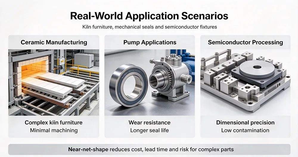
SiSiC Across Applications
7. Common Misconceptions About Near-Net-Shape SiSiC
7.1 "Near-Net-Shape Means No Machining Is Needed"
Near-net-shape does not mean zero machining. While the process minimizes the need for machining, some finishing is usually required to achieve the final surface finish and tolerances. The key advantage is that the amount of machining is significantly reduced compared to conventional ceramics.7.2 "Near-Net-Shape Works for All Ceramics"
Near-net-shape forming is not unique to Reaction-Bonded Silicon Carbide (SiSiC) , but it is particularly well-suited to this material because of its reaction bonding process. Other ceramics, such as alumina and silicon nitride, can also be near-net-shape formed, but the shrinkage is typically higher and the process is more difficult to control.7.3 "Near-Net-Shape Is Only for Simple Shapes"
Near-net-shape forming is actually most valuable for complex shapes. Simple shapes can often be machined from standard blanks, but complex shapes with internal features, curves, and fine details are difficult or impossible to machine. Near-net-shape forming allows these complex shapes to be produced directly.7.4 "Near-Net-Shape SiSiC Is More Expensive"
While Reaction-Bonded Silicon Carbide (SiSiC) may have a higher initial material cost than some conventional ceramics, the total cost of ownership is often lower because of reduced machining, less material waste, and shorter lead times. For complex components, the cost savings can be significant.7.5 "Near-Net-Shape Eliminates Design Constraints"
Near-net-shape forming reduces design constraints but does not eliminate them. There are still limits to the complexity and size of components that can be produced, and the design must be compatible with the reaction bonding process. Designers should work closely with the manufacturer to optimize component geometry.8. Quick Evaluation Checklist
Before selecting Reaction-Bonded Silicon Carbide (SiSiC) for your application, verify the following key parameters:Maximum operating temperature (1380°C in air)
Atmosphere (air, inert, reducing, vacuum)
Chemical compatibility with the process material
Thermal shock resistance requirements
Mechanical load and wear conditions
Component size and shape complexity
Surface finish and tolerance requirements
Machining requirements
Quality control and inspection requirements
Supplier capability and technical support
9. Real-World Application Scenarios
9.1 SiSiC Kiln Furniture in Ceramic Manufacturing
A ceramic manufacturer replaced traditional cordierite kiln furniture with Reaction-Bonded Silicon Carbide (SiSiC) setters and beams. The near-net-shape capability allowed complex kiln furniture geometries to be produced with minimal machining, reducing cost and lead time. The Reaction-Bonded Silicon Carbide (SiSiC) components also offered higher thermal conductivity, better thermal shock resistance, and longer service life.9.2 SiSiC Mechanical Seals in Pump Applications
A pump manufacturer selected Reaction-Bonded Silicon Carbide (SiSiC) for mechanical seal rings. The near-net-shape capability allowed complex seal geometries to be produced with minimal machining, while the high hardness and wear resistance of Reaction-Bonded Silicon Carbide (SiSiC) extended seal life and reduced maintenance costs.9.3 SiSiC Components in Semiconductor Processing
A semiconductor equipment manufacturer used Reaction-Bonded Silicon Carbide (SiSiC) for wafer processing fixtures. The near-net-shape capability allowed complex wafer handling geometries to be produced with minimal contamination risk. The high purity and chemical inertness of Reaction-Bonded Silicon Carbide (SiSiC) ensured consistent process performance.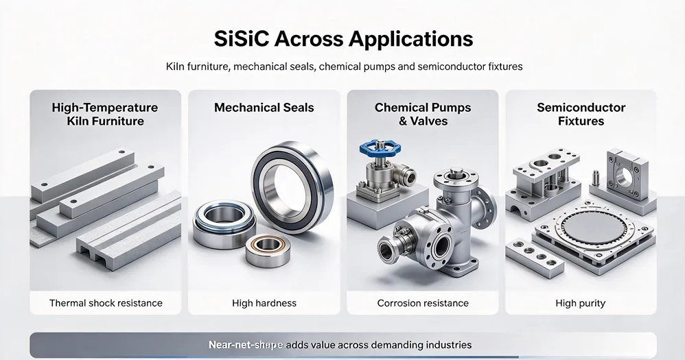
SiSiC Across Applications
10. Frequently Asked Questions (FAQs)
Q1: What is the main difference between RB-SiC and Sintered Silicon Carbide (SSiC)?The key difference is the manufacturing process. RB-SiC is densified via a chemical reaction with molten silicon, resulting in minimal shrinkage and containing some free silicon. SSiC is sintered without a chemical reaction, is nearly 100% SiC, and generally offers higher room-temperature strength and better corrosion resistance but is less suitable for large, complex shapes.
Q2: Why is the maximum use temperature of RB-SiC limited to around 1380°C?
This limitation is due to the residual free silicon (melting point 1414°C) within the microstructure. Prolonged exposure in air above 1380°C can cause the silicon to oxidize or soften, leading to a degradation of mechanical properties.
Q3: In which chemical environments is RB-SiC not suitable?
RB-SiC is not recommended for use in hydrofluoric acid (HF) or hot, concentrated alkaline solutions, as the free silicon phase will react and corrode.
Q4: What does "Near-Net-Shape" mean, and what is the benefit?
"Near-Net-Shape" means the final product is formed very close to its desired dimensions. For RB-SiC, the sintering shrinkage is less than 1%, so the final part closely matches the mold. This drastically reduces the need for and cost of extensive final machining.
Q5: Is RB-SiC a good electrical insulator?
No, Silicon Carbide is a semiconductor. The presence of free silicon, which is metallic, further increases the electrical conductivity of RB-SiC compared to the pure SSiC variety. It is not typically used as an insulator.
Leave a Reply
Your email address will not be published.Required fields are marked. *