Overview of Direct Copper Plated Substrate
Direct Copper Plated Substrate is an advanced electronic packaging technology. It forms a high-quality conductive layer by directly plating a layer of copper on the surface of a ceramic, metal, or composite substrate. This technology has high electrical conductivity, low resistivity, and good thermal conductivity, which can effectively improve the thermal and electrical performance of electronic devices. At the same time, the direct copper plated substrate process is simple, relatively low cost, widely used in semiconductor packaging, electronic circuit manufacturing and other fields, for the development and production of high-performance electronic products to provide important support.

Direct Copper Plated Substrate
Features of Direct Copper Plated Substrate
Direct Copper Plated Substrate is a widely used technology in the field of electronic packaging, and its features are remarkable. Firstly, it has excellent conductivity; the copper layer has very low resistivity, which can effectively reduce the energy consumption of the circuit and improve the signal transmission efficiency. Secondly, its high thermal conductivity can quickly conduct heat and effectively solve the problem of heat accumulation in the working process of electronic devices.
In addition, the direct copper plating substrate adhesion is strong, the combination between the copper layer and the substrate is strong, not easy to peel off, even in high temperature, high humidity and other harsh environments, can maintain good performance. Process, direct copper plating technology is relatively simple, easy to operate, low cost, and easy to mass production.
These features make Direct Copper Plated Substrate a vital component in semiconductor packaging, electronic circuit manufacturing, optoelectronic devices, and other fields, supporting the high performance and miniaturization of electronic products.
Specifications Table of Direct Copper Plated Substrate
|
Applications of Direct Copper Plated Substrate
In electronic packaging, Direct Copper Plated Substrate is a key material for semiconductor chip packaging. Its high conductivity and low resistivity reduce power loss and improve signal transmission speed and stability. Its thermal conductivity also ensures stable chip operation in high-temperature environments. For instance, it is widely used in high-performance computing and 5G communication chip packaging.
In electronic circuit manufacturing, it enables the production of multilayer printed circuit boards (PCBs), with the copper layer serving as conductive lines for complex circuits. Its flatness and uniformity enhance PCB manufacturing accuracy and reliability.
In the field of new energy, the direct copper plating substrate also plays an important role. For example, in the power module package of electric vehicles, its high conductivity and heat dissipation performance can effectively improve the performance of the power module to meet the demand for high power density and high reliability of electric vehicles. In addition, in the manufacture of solar panels, direct copper-plated substrates can be used to make electrodes to improve the photoelectric conversion efficiency and stability of the panel.
Company Profile
Luoyang Tongrun Nano Technology Co. Ltd. (TRUNNANO) is a trusted global chemical material supplier & manufacturer with over 12-year-experience in providing super high-quality chemicals and nanomaterials, including boride powder, nitride powder, graphite powder, ceramic products, 3D printing powder, etc.
The company has a professional technical department and Quality Supervision Department, a well-equipped laboratory, and equipped with advanced testing equipment and after-sales customer service center.
If you are looking for high-quality Ceramic Products please feel free to contact us or click on the needed products to send an inquiry.
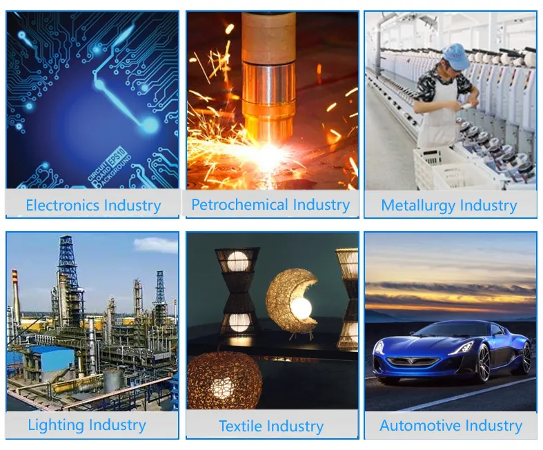
Applications of Ceramic Products
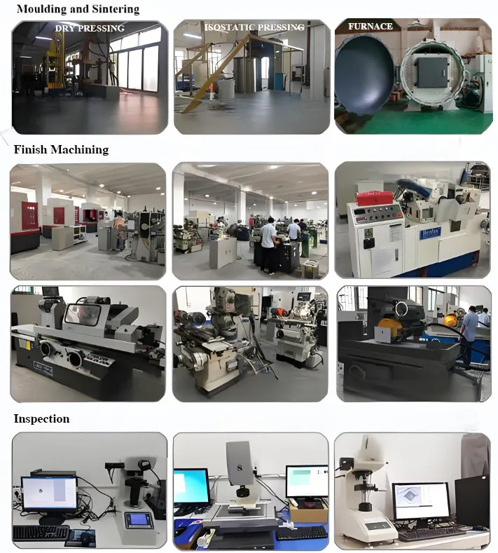
Process of Ceramic Products
Payment Term
T/T, Western Union, Paypal, Credit Card etc.
Shipment Term
By air, by sea, by express, as customers request.
5 FAQs of Direct Copper Plated Substrate
Q1: What is the process flow of Direct Copper Plated Substrate?
The process flow of Direct Copper Plated Substrate (using DPC ceramic substrate as an example) typically includes the following steps: First, the ceramic substrate is pre-treated, such as cleaning. Then, laser drilling is used to create through holes (with aperture diameters generally ranging from 60 μm to 120 μm). Next, a metal seed layer is deposited on the substrate surface using magnetron sputtering (with a Ti/Cu target). Photolithography and development are then used to form the circuit patterns. Electroplating is used to fill the holes and thicken the metal lines. Finally, surface treatment improves solderability and oxidation resistance, and the dry film is removed, followed by etching the seed layer to complete the substrate.
Q2: What are the advantages and disadvantages of Direct Copper Plated Substrate compared to other ceramic metallization technologies like DBC and AMB?
Advantages: Direct Copper Plated Substrate offers high line accuracy, with line width and spacing as low as 30 μm to 50 μm, meeting the precision requirements of microelectronic packaging. Laser drilling and plating allow vertical interconnections between the upper and lower surfaces of the ceramic substrate. The low-temperature process (below 300°C) avoids thermal damage to the substrate and metal lines.
Disadvantages: The electroplating process used to create the metal lines can cause significant environmental pollution. Electroplating growth is slow, limiting the line thickness. The bonding strength between the metal layer and ceramics is relatively weak, affecting product reliability.
Q3: What are the application areas of Direct Copper Plated Substrate?
Direct Copper Plated Substrate is widely used in high-power LED lighting, such as automotive headlights and plant lighting. Its high thermal conductivity, precision, and flatness effectively address LED heat dissipation issues, reduce device size, and ensure long-term stable operation. In semiconductor lasers, it serves as a substrate material, enhancing heat dissipation and reducing thermal resistance to increase laser output power and lifespan. It is also used in emerging fields like LIDAR, optical communication, power semiconductor packaging, and RF microwave device packaging.
Q4: Is the cost of the Direct Copper Plated Substrate high?
The production of Direct Copper Plated Substrate involves complex processes such as semiconductor microfabrication (e.g., sputtering, photolithography) and printed circuit board preparation. These processes require precise material control and process integration, resulting in relatively high product costs.
Q5: What is the future development trend of Direct Copper Plated Substrate technology?
In the future, advancements in Direct Copper Plated Substrate technology are expected to focus on improving the bonding strength between the metal layer and ceramic substrate, optimizing the plating process to reduce costs and enhance production efficiency, and minimizing environmental impact. As electronic devices continue to evolve towards miniaturization, high performance, and high integration, Direct Copper Plated Substrate is poised to play a significant role in emerging fields such as artificial intelligence, the Internet of Things, 5G communications, and new energy vehicles, with a promising market outlook.