Overview of Direct bonding to copper substrates
Direct bonding to copper substrates represents an advanced electronic packaging technology that directly connects copper substrates to chips or other substrates using specialized bonding materials or processes. By streamlining the packaging structure and reducing package size, this technology is particularly suited for high-power, high-density electronic device packaging. Widely employed in semiconductor and microelectronic fields, it meets the demand for high-performance packaging in modern electronic equipment.
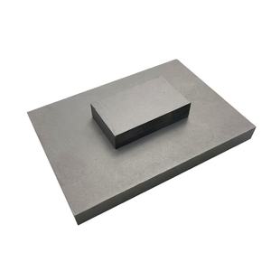
Direct bonding to copper substrates
Key Features of Direct Bonded Copper (DBC)
Excellent heat dissipation: The extremely high thermal conductivity of copper enables it to conduct heat quickly, effectively lowering the operating temperature of the chip and improving the stability and life of the device.
High Reliability: Via high-temperature and high-pressure processes, the copper layer forms a strong metallurgical bond with ceramic substrates (such as alumina or aluminum nitride), offering robust mechanical strength and thermal shock resistance. This allows it to withstand extreme temperature fluctuations and mechanical stress.
Good electrical insulation: The ceramic substrate provides good electrical insulation, preventing short circuits and leakage and ensuring the safe operation of the circuit.
Precise line patterning: The copper layer allows for high-precision patterning to meet the needs of complex circuit design and is suitable for high-density, high-performance electronic packaging.
Adaptability: DBC substrates can be utilized for various power semiconductor devices, such as IGBTs and MOSFETs, and find extensive applications in power electronics, new energy vehicles, and 5G communications.
Environmentally Friendly and Lead-Free: The manufacturing process typically involves no lead or other hazardous substances, aligning with environmental standards.
Specification Table for Direct Bonded Copper Substrates
| Parameter |
Description |
Typical Values |
| Material Composition |
Base material and copper layer |
- Ceramic: Alumina (Al₂O₃), Aluminum Nitride (AlN), Silicon Nitride (Si₃N₄)
- Copper purity: >99.9% |
| Ceramic Thickness |
Thickness of the ceramic substrate |
- Alumina: 0.25 mm to 3.0 mm
- Aluminum Nitride: 0.3 mm to 6.0 mm
- Silicon Nitride: 0.5 mm to 10 mm |
| Copper Thickness |
Thickness of the copper layer |
- Single layer: 100 µm to 400 µm
- Double layer: 200 µm to 800 µm (total) |
| Thermal Conductivity |
Ability to conduct heat |
- Alumina: 20 - 35 W/(m·K)
- Aluminum Nitride: 170 - 220 W/(m·K)
- Silicon Nitride: 80 - 120 W/(m·K) |
| Thermal Expansion Coefficient |
Coefficient of thermal expansion (CTE) |
- Alumina: 6.5 - 7.5 ppm/K
- Aluminum Nitride: 4.5 - 5.0 ppm/K
- Silicon Nitride: 3.0 - 3.5 ppm/K |
| Dielectric Strength |
Electrical insulation capability |
- Alumina: >15 kV/mm
- Aluminum Nitride: >10 kV/mm
- Silicon Nitride: >10 kV/mm |
| Bonding Temperature |
Temperature required for bonding copper to ceramic |
- Alumina: 1065°C - 1085°C
- Aluminum Nitride: 1065°C - 1085°C
- Silicon Nitride: 1065°C - 1085°C |
| Bonding Pressure |
Pressure applied during bonding process |
- Typically 1 - 10 MPa (varies with material and thickness) |
| Surface Roughness |
Roughness of the copper surface |
- Ra: 0.1 µm to 1.0 µm (typically controlled for good bonding) |
| Adhesion Strength |
Strength of the bond between copper and ceramic |
- Typically > 30 MPa (shear strength) |
| Operating Temperature Range |
Temperature range for stable operation |
- -55°C to +200°C (depending on application) |
| Maximum Power Density |
Maximum power density that can be handled |
- Varies widely based on application and cooling system; typically up to 100 W/cm² for high-power devices |
| Surface Finish |
Final surface treatment of copper layer |
- Electroplated, chemically etched, or polished as required for specific applications |
|
Applications of Direct-Bonded Copper Substrates
Direct Bond Copper (DBC) substrates are high-performance packaging materials with widespread applications, especially in scenarios where thermal dissipation and reliability are critical.
Power Electronics: DBC substrates are ideal for packaging power semiconductor devices like IGBTs, MOSFETs, and diodes used in power conversion and motor drives. These devices generate significant heat during operation.
New Energy Vehicles: Core components of new energy vehicles, such as electric drive systems and charging stations, have stringent requirements for thermal dissipation and reliability. DBC substrates meet the operational demands of these components in high-temperature, high-humidity, and high-vibration environments, ensuring power device efficiency and enhancing vehicle performance and safety.
5G Communications: Key components of 5G base stations, such as RF power amplifiers and filters, require efficient thermal dissipation and reliable packaging. DBC substrates, with their high thermal conductivity and excellent electrical insulation properties, fulfill the thermal dissipation and electrical isolation needs of 5G equipment under high-frequency, high-power conditions, safeguarding stable communication equipment operation.
Industrial Automation: In industrial automation equipment, like robots and industrial motor drives, DBC substrates are used to package power modules. This ensures equipment maintains high efficiency and stability during long-term, high-load operation.
Aerospace and Military: Due to their high reliability, temperature resistance, and mechanical shock resistance, DBC substrates are suitable for aerospace and military electronic equipment, such as radar, satellite communications, and flight control systems. They can withstand extreme environmental conditions and protect critical equipment from instability.
Company Profile
Luoyang Tongrun Nano Technology Co. Ltd. (TRUNNANO) is a trusted global chemical material supplier & manufacturer with over 12-year-experience in providing super high-quality chemicals and nanomaterials, including boride powder, nitride powder, graphite powder, ceramic products, 3D printing powder, etc.
The company has a professional technical department and Quality Supervision Department, a well-equipped laboratory, and equipped with advanced testing equipment and after-sales customer service center.
If you are looking for high-quality Ceramic Products please feel free to contact us or click on the needed products to send an inquiry.
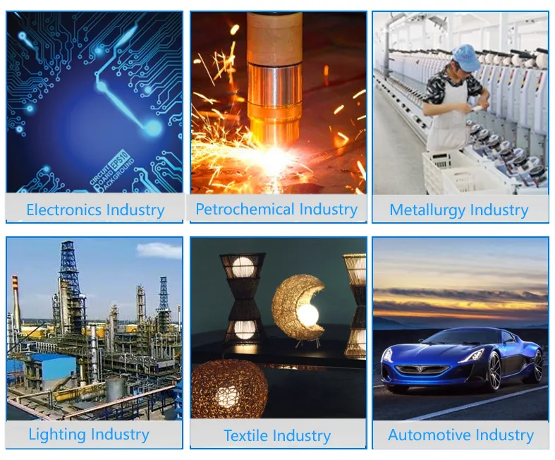
Applications of Ceramic Products
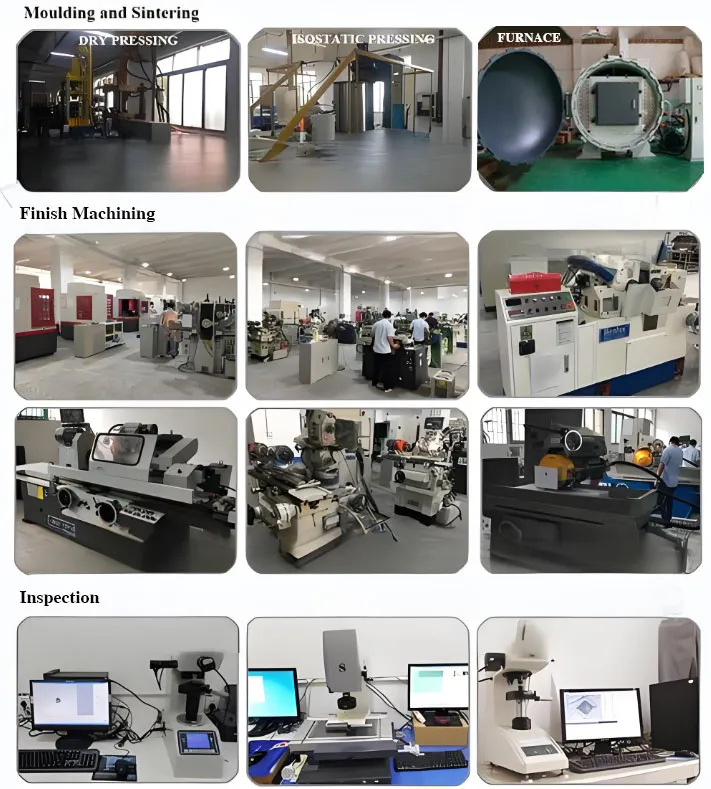
Process of Ceramic Products
Payment Term
T/T, Western Union, Paypal, Credit Card etc.
Shipment Term
By air, by sea, by express, as customers request.
5 FAQs About Direct Bonded Copper Substrates
Q1: What is the basic principle of direct-bonded copper substrates?
Direct bonded copper substrates are composite substrates formed by directly bonding a pure copper layer to a ceramic insulator (e.g., alumina or aluminum nitride) through a high-temperature melting and diffusion process. The principle is based on the metallurgical combination of copper and ceramics formed at high temperature, which makes the copper layer and ceramic substrate tightly bonded with both the high electrical conductivity of copper and ceramic, high thermal conductivity, high electrical insulation, and other characteristics.
Q2: What is the thermal conductivity of DBC substrates?
The thermal conductivity of DBC substrates varies depending on the ceramic substrate material used. Common alumina ceramic copper clad laminates have a thermal conductivity of 15W~35W/(m・K), aluminum nitride ceramic copper clad laminates have a thermal conductivity of 170W~260W/(m・K), and silicon nitride ceramic copper clad laminates have a thermal conductivity of 80W~120W/(m・K). These materials all exhibit high thermal conductivity, meeting the thermal dissipation requirements of high-power applications.
Q3: What is the coefficient of thermal expansion of DBC substrates?
The coefficient of thermal expansion (CTE) of DBC substrates varies with the material. Alumina DBC has a CTE of 7.1 ppm/K, while aluminum nitride DBC has a CTE of 4.7 ppm/K, which is close to that of silicon (4 ppm/K). This reduces thermal stress caused by CTE mismatches when bonding with semiconductor devices such as chips.
Q4: What are the fabrication methods for DBC substrates?
Common fabrication methods for DBC substrates include direct bonding and active metal brazing (AMB). Direct bonding involves attaching copper foil directly to the ceramic substrate surface at high temperatures. Active metal brazing utilizes active metal elements in the solder to bond ceramics and metals.
Q5: What are the key process parameters in DBC substrate fabrication?
In the direct bonding process, key parameters include bonding temperature, pressure, and time. Typically, the bonding temperature must exceed copper's melting point, usually above 1064°C. Pressure is adjusted based on the ceramic substrate's size and thickness to ensure sufficient contact and bonding between the copper layer and ceramic substrate.