In the fast-evolving worlds of semiconductor manufacturing, MEMS devices, power electronics, and integrated photonics, material performance directly defines product reliability, efficiency, and lifespan. Among advanced substrate and thin-film materials, silicon nitride (SiN) wafers stand out as a high-performance solution that combines robust mechanical strength, excellent electrical insulation, and outstanding thermal stability. Unlike conventional silicon, silicon dioxide, or many ceramic substrates, SiN maintains its key properties under harsh conditions—high temperatures, rapid thermal cycling, mechanical stress, corrosive chemicals, and high electric fields.
This article explores the core properties of SiN wafers, with a focus on mechanical strength, electrical insulation, and thermal stability. We explain the science behind these characteristics, compare SiN with competing materials, and outline real-world applications where these properties solve critical engineering challenges. For engineers, researchers, and procurement specialists working in high-tech industries, understanding SiN’s fundamental properties is essential to selecting the right substrate for next-generation devices.
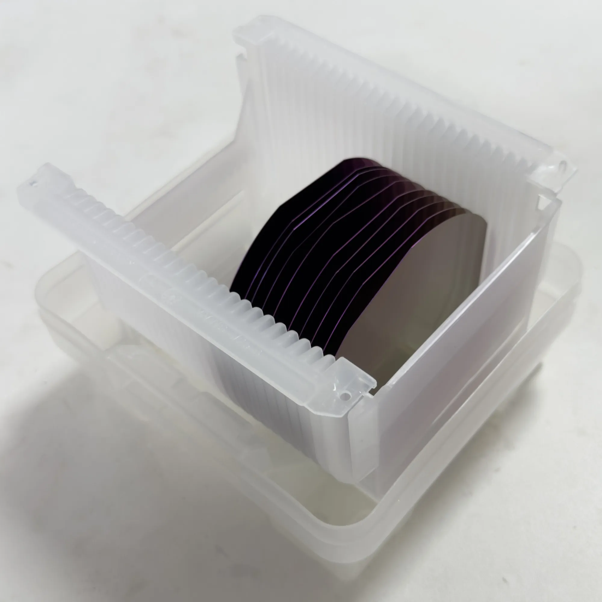
Silicon Nitride Wafer
Silicon nitride wafers are advanced ceramic substrates or silicon wafers coated with a high-quality silicon nitride (Si₃N₄ or SiNₓ) thin film. They are produced through precision deposition processes—most commonly LPCVD (Low-Pressure Chemical Vapor Deposition) and PECVD (Plasma-Enhanced Chemical Vapor Deposition)—which allow tight control over thickness, stress, uniformity, and stoichiometry. SiN is a covalently bonded compound with a strong atomic structure, giving it intrinsic resistance to heat, mechanical damage, and electrical breakdown.
SiN wafers are manufactured in several forms to suit diverse applications: bulk SiN wafers are solid ceramic substrates for high-power and high-temperature modules; SiN-coated silicon wafers are standard Si wafers with a protective or functional SiN layer; low-stress SiN films are optimized for MEMS, optical waveguides, and precision sensors; and high-stress SiN films are used for structural reinforcement and mechanical components. Due to their versatility, SiN wafers are widely used in semiconductor integrated circuits (ICs), micro-electro-mechanical systems (MEMS), power electronics (IGBT, MOSFET, SiC modules), integrated photonics and optical communications, medical devices and biosensors, and aerospace and industrial electronics. The unique combination of strength, insulation, and thermal stability makes SiN a preferred material where ordinary substrates fail.
Mechanical performance is one of the most celebrated advantages of silicon nitride. SiN exhibits high hardness, high flexural strength, excellent fracture toughness, and resistance to wear and mechanical shock—far exceeding many traditional ceramics and silicon-based materials. Its flexural (bending) strength is typically above 700–800 MPa, and in high-density sintered bulk substrates, it can exceed 1000 MPa, which is roughly three times higher than alumina (Al₂O₃) and significantly stronger than standard silicon. Its Vickers hardness ranges from 800 to 1000 kgf/mm², making SiN one of the hardest engineering ceramics, translating to exceptional wear resistance ideal for durable components, protective coatings, and long-life mechanical structures.
A major limitation of many ceramics is brittleness, but SiN solves this with fracture toughness values of 6.5–7 MPa·m¹ᐟ²—more than double that of aluminum nitride (AlN) and far better than alumina. High fracture toughness means SiN resists cracking, chipping, and catastrophic failure under mechanical stress or impact, which is critical for thin MEMS membranes and cantilevers, power modules exposed to vibration and thermal stress, devices undergoing dicing, polishing, and assembly, and portable and rugged electronics. Unlike many metals and polymers that soften at high temperatures, SiN retains its strength up to 1000°C–1200°C without significant degradation; it does not melt but decomposes at approximately 1800°C–1900°C, allowing use in extreme thermal environments.
For SiN thin films deposited on silicon wafers, stress control is vital. Manufacturers can produce low-stress SiN (near-zero or mild tensile stress ±300 MPa) for photonics, passivation, and delicate MEMS, as well as high-stress SiN (tensile stress up to 800–900 MPa) for structural rigidity and mechanical components. This tunability makes SiN extremely versatile for microfabrication. In industrial and consumer electronics, mechanical failure leads to downtime, safety risks, and product recalls, so SiN’s strength enables thinner, lighter, and more compact device designs, higher reliability under shock, vibration, and physical stress, longer service life in harsh environments, and compatibility with high-precision manufacturing processes.
SiN is an excellent dielectric material with outstanding electrical insulation performance, widely used as an isolation layer, passivation film, and barrier in high-voltage and high-frequency electronic systems. It features a dielectric breakdown strength of 8–10 MV/cm (80–100 kV/mm) for thin films, and bulk substrates can achieve 20–25 kV/mm, allowing SiN to withstand high voltages without arcing or failure—ideal for power electronics and high-voltage semiconductors. At room temperature, SiN has a volume resistivity greater than 10¹⁴ Ω·cm, effectively blocking current leakage, and even at elevated temperatures, it maintains strong insulating behavior—unlike many polymers that lose insulation at high heat.
SiN has a dielectric constant around 7.0–7.5, higher than silicon dioxide (SiO₂), making it useful for capacitor dielectrics, gate insulation, interlayer dielectric (ILD) in ICs, and impedance matching in high-frequency circuits. Its leakage current is typically below 10⁻⁹ A/cm² under normal operating conditions, supporting energy efficiency and stable device performance. Beyond basic insulation, SiN acts as a superior barrier against moisture and ionic contaminants, oxygen diffusion, alkali ions (e.g., Na⁺) that cause device drift, and plasma and chemical etching damage. As a passivation layer, SiN significantly improves device reliability and lifespan.
These electrical insulation properties make SiN wafers indispensable in a range of applications, including power semiconductor modules (EV, industrial inverters), high-voltage sensors and detectors, integrated circuits and multi-chip modules, isolation layers in MEMS and photonics, and harsh-environment industrial electronics. In high-power systems, where electrical safety and stability are paramount, SiN’s insulation capabilities prevent short circuits, reduce energy loss, and ensure long-term device operation.
Thermal stability defines a material’s ability to resist deformation, degradation, or property change under heat and rapid temperature change, and SiN excels in high operating temperatures, low thermal expansion, good thermal conductivity, and exceptional thermal shock resistance. SiN performs reliably from cryogenic temperatures up to 1000°C–1300°C; it does not soften, creep, or deform under long-term high-temperature exposure, unlike many plastics, epoxies, and even some metals. Its thermal expansion coefficient (CTE) of approximately 3.0–3.2 × 10⁻⁶ /°C is closely matched to silicon (Si) and silicon carbide (SiC), minimizing thermal stress during heating and cooling, which reduces warping, cracking, and delamination in bonded structures.
Bulk SiN substrates offer thermal conductivity of 90–120 W/(m·K), efficiently dissipating heat from high-power chips. While slightly lower than AlN, SiN provides a far better balance of thermal performance and mechanical toughness. SiN also withstands rapid temperature fluctuations without failure, surviving repeated thermal cycling between –50°C and 800°C—a critical advantage in power electronics, aerospace, and automotive systems. At elevated temperatures, SiN forms a thin protective oxide layer that resists further oxidation, and it is chemically inert against most acids, alkalis, and solvents—except concentrated HF and hot phosphoric acid—making it suitable for corrosive and high-temperature industrial environments.
Thermal stability is critical for reducing failure in high-power devices, extending lifetime under thermal cycling, improving efficiency in high-temperature environments, enabling miniaturization without overheating, and supporting harsh-environment applications (oil, gas, aerospace, automotive). As devices become more powerful and compact, the demand for materials with superior thermal stability continues to grow, and SiN wafers meet this need by maintaining consistent performance even in the most extreme thermal conditions.
To fully appreciate SiN’s advantages, it is helpful to compare it with widely used substrates. Silicon (Si), the most common semiconductor material, offers good thermal conductivity but is conductive when doped and lacks the mechanical strength and insulation of SiN. Alumina (Al₂O₃) is a low-cost ceramic option but has low flexural strength, poor fracture toughness, and low thermal conductivity, making it unsuitable for high-reliability applications. Aluminum Nitride (AlN) has excellent thermal conductivity and good insulation but is brittle and has poor thermal shock resistance, limiting its use in harsh environments.
SiN stands out by providing the best overall balance of strength, insulation, and thermal stability. It outperforms AlN in toughness and thermal shock, outperforms alumina in nearly every category, and offers insulation that bulk silicon cannot match. This balance makes SiN the preferred choice for applications where reliability, durability, and performance are non-negotiable—from high-power electronics to MEMS sensors and aerospace components.
SiN’s unique combination of strength, insulation, and thermal stability unlocks innovation across industries. In semiconductors and integrated circuits, SiN is used as passivation layers, hard masks for etching, gate dielectrics, and device isolation and moisture barriers, improving device reliability and lifespan. In MEMS and sensors, SiN’s mechanical strength and low stress make it ideal for pressure sensors, accelerometers, gyroscopes, micro-mirrors, optical switches, and durable mechanical membranes, enabling precise and reliable operation in harsh conditions.
In power electronics and electric vehicles, SiN wafers are used in IGBT and SiC module substrates, high-voltage insulation, thermal management layers, and inverter and converter components, supporting the shift to more efficient and compact power systems. In integrated photonics and optoelectronics, low-loss SiN films enable optical waveguides, couplers, splitters, and high-stability photonic chips, advancing optical communication technology. In industrial and aerospace electronics, SiN’s ruggedness makes it suitable for rugged sensors, high-temperature controls, satellite and avionic systems, and oil-gas drilling equipment. Even in medical devices, SiN’s biocompatibility and chemical inertness make it ideal for biosensors, implantable components, lab-on-a-chip systems, and biocompatible microfluidics.
Silicon nitride (SiN) wafers are a cornerstone of modern high-tech engineering, thanks to their unrivaled combination of mechanical strength, electrical insulation, and thermal stability. From consumer electronics to electric vehicles, from industrial sensors to satellite systems, SiN enables devices that are smaller, more efficient, and more reliable than ever before. Its high flexural strength and fracture toughness resist mechanical failure; its excellent dielectric properties ensure safe electrical isolation; its outstanding thermal stability withstands extreme heat and rapid temperature change. Together, these properties make SiN not just a substrate material, but a performance enabler for next-generation technology.
For anyone involved in semiconductor manufacturing, MEMS, power electronics, or photonics, selecting SiN wafers means investing in long-term durability, consistent performance, and design freedom. As industry demands continue to rise—for smaller, more powerful, and more rugged devices—silicon nitride will remain at the forefront of advanced materials innovation, driving progress across high-tech sectors worldwide.
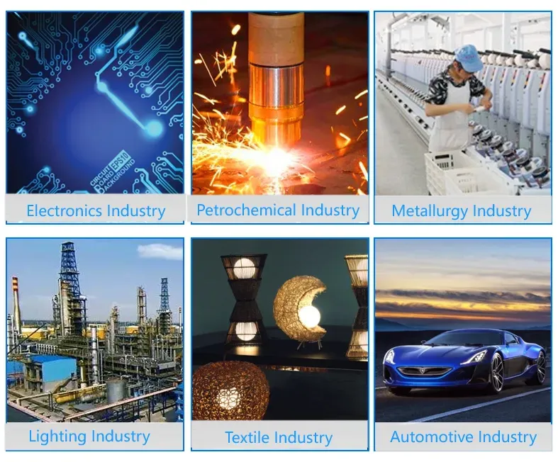
Application of Silicon Nitride Wafer
Q1: What is the difference between Si₃N₄ and SiNₓ wafers? A: Si₃N₄ refers to stoichiometric silicon nitride, while SiNₓ denotes non-stoichiometric films with variable silicon-to-nitrogen ratios. Both are commonly called SiN wafers in industry, with SiNₓ being more flexible for custom applications.
Q2: Are SiN wafers suitable for high-temperature applications? A: Yes. SiN maintains stability up to 1000°C–1300°C and resists oxidation and thermal shock, making it ideal for high-temperature industrial and aerospace applications.
Q3: Can SiN replace AlN in power modules? A: In many cases, yes. SiN offers lower fracture risk and better thermal shock resistance, while providing sufficient thermal conductivity for most power module applications.
Q4: Are SiN wafers biocompatible? A: Yes, SiN is chemically inert and non-toxic, making it widely used in medical and biosensor applications, including implantable devices and lab-on-a-chip systems.
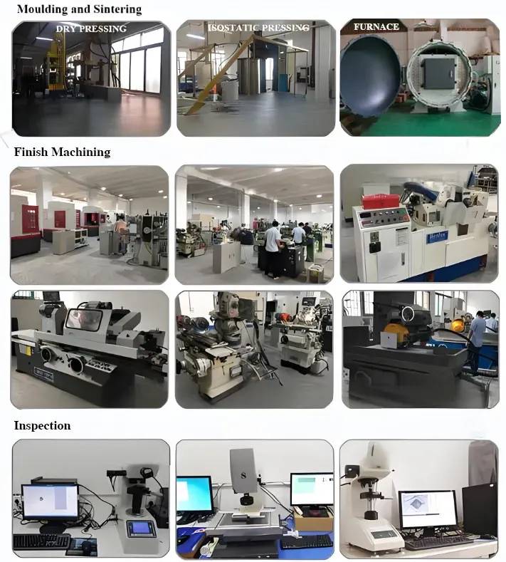
Q5: What processes are used to make SiN wafers? A: LPCVD and PECVD are the most common processes for thin-film SiN wafers, while bulk SiN substrates are produced through high-temperature sintering for maximum strength and thermal stability.