The Difference Between Hexagonal Boron Nitride and Cubic Noron Nitride
Views : 1919
Update time : 2022-01-27 10:26:32
The Difference Between Hexagonal Boron Nitride and Cubic Noron Nitride
Boron nitride is a crystal composed of nitrogen atoms and boron atoms. The chemical composition is 43.6% boron and 56.4% nitrogen with four different variants: hexagonal boron nitride (HBN), cubic boron nitride (CBN), rhombohedral boron nitride (RBN) and wurtzite nitrogen Boronide (WBN). Among them, hexagonal boron nitride and cubic boron nitride are more commonly used. Boron nitride is mainly used in refractory materials, semiconductor solid-phase doping sources, structural materials of atomic stacks, packaging materials against neutron radiation, rocket engine components, high-temperature lubricants and mold release agents. Fibers processed with boron nitride can be used as inorganic synthetic engineering materials and are widely used in aerospace and defense industries. CBN can also be used as deep well drill bits and high-speed cutting tools.
Hexagonal boron nitride
What is the difference between hexagonal boron nitride and cubic boron nitride?
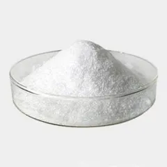
Hexagonal Boron Nitride: Hexagonal boron nitride (similar to graphite, also known as graphite boron nitride, white graphite). Relative density 2.25. The Mohs hardness is about 2. It is a white powder that melts at about 3000°C under high pressure. Has good electrical insulation, thermal conductivity, corrosion resistance and good lubricity. It has good chemical stability and does not react with water, acid and alkali at room temperature. Reacts with hot concentrated or molten alkali and hot chlorine gas. Can withstand 2000 ℃ high temperature. Has a strong ability to withdraw electrons. It can be obtained by heating borax and ammonium chloride in a stream of ammonia.
BN and graphite are isoelectronic bodies. It is known as white graphite, has a layered structure similar to graphite, has good lubricity, electrical insulation, thermal conductivity and chemical resistance, and has neutron absorption ability. Chemically stable and chemically inert to all molten metals, shaped products are easy to machine and have high moisture resistance. The melting point is 3000°C under nitrogen pressure, and it sublimates at 2500°C under atmospheric pressure. Its theoretical density is 2.29 grams per cubic centimeter. Mohs hardness of 2, anti-oxidation temperature of 900 ° C, high temperature resistance of 2000 ° C, the melting point of use in nitrogen and argon is 3000 ° C. It is a chemically inert material and is stable up to 2700°C under an argon atmosphere.
Cubic Boron Nitride: Cubic boron nitride (diamond type). For black or brown granular crystals. Relative density 3.48. Melting point 3000 ℃. The hardness is comparable to that of diamond. Stability at high temperature is better than diamond. Boron and nitrogen can be directly synthesized under high temperature and high pressure conditions.
cubic boron nitride
Boron nitride with cubic structure: the molecular formula is BN, its crystal structure is similar to that of diamond, and its hardness is slightly lower than that of diamond, which is HV72000-98000 MPa, and is often used as abrasive and tool material. In 1957, R.H. Wintorf of the United States first developed the cube. In 2013, Yanshan University successfully synthesized a new material of cubic boron nitride with nano-twin structure. This new material has a variety of excellent characteristics. Its hardness is higher than that of diamond single crystal, its toughness is better than that of commercial cemented carbide, and its oxidation resistance temperature is higher than that of cubic boron nitride single crystal itself. It is expected to become a new generation tool material in the steel material processing industry. Has broad application prospects.
The core difference between cubic boron nitride and hexagonal boron nitride is that the physical structure is different. The crystal form of cubic boron nitride is more pressure-resistant and wear-resistant, and is often used in cutting tools. The price is relatively low. , Selling at a low price, it is a concept of stealing. Although the main chemical composition of this kind of coating is also boron nitride, the actual non-stick effect of aluminum is not good.
Another crystal form of boron nitride is hexagonal boron nitride. This crystal form of boron nitride has super lubricating function, high temperature resistance, and metal non-wetting. It is the preferred material for high temperature non-stick aluminum coatings, and the price is relatively expensive. The best non-stick aluminum effect on the market is mainly this boron nitride coating.
Continuation: A Detailed Comparison of Properties, Synthesis Methods, and Advanced Applications Having established the fundamental structural distinction between hexagonal boron nitride (hBN) and cubic boron nitride (cBN), a deeper exploration of their contrasting properties, synthesis pathways, and the resulting specialized applications reveals why these two polymorphs occupy such critical yet disparate roles in advanced technology.
hexagonal boron nitride
Property Analysis: Beyond Hardness and Lubricity While hardness and lubricity are the most cited differentiating properties, the divergence in their electronic, thermal, and optical characteristics is equally significant.
Thermal Conductivity and Management hBN: Often called the "white graphene," hBN exhibits exceptionally high in-plane thermal conductivity (up to ~400-600 W/m·K in high-quality flakes), rivaling that of graphene, while being an excellent electrical insulator. This unique combination makes it an ideal substrate, filler, or coating material for thermal management in high-power electronics, such as transistors and LEDs, where heat must be dissipated without creating electrical shorts. Its anisotropic thermal conduction (high in-plane, lower through-plane) is also exploited in composite materials. cBN:It also possesses high thermal conductivity (~13 W/m·K, which is high for a ceramic but lower than hBN's in-plane value). However, its paramount feature in this domain is its thermal stability in oxidizing environments. Unlike diamond, which oxidizes above ~600°C, cBN remains stable up to ~1400°C in inert or vacuum conditions and resists oxidation better. This allows cBN cutting tools to maintain their integrity at very high machining temperatures where diamond would degrade.
Electronic and Optical Properties hBN: With a wide indirect bandgap (~6 eV), hBN is a deep ultraviolet (UV) dielectric material. It is a cornerstone of van der Waals (vdW) heterostructures in 2D material research, serving as an atomically flat, charge-trapping-free insulating substrate or encapsulation layer for graphene, transition metal dichalcogenides (like MoS₂), and other 2D semiconductors. Its low dielectric constant and absence of dangling bonds dramatically improve the electronic mobility and performance of these devices. cBN: It has a similarly wide indirect bandgap (~6.4 eV). Research into its potential as a UV emitter or detector is ongoing, but its primary electronic application leverages its extreme hardness and insulating properties: as a durable dielectric coating or in high-temperature, high-power electronic devices where structural robustness is key.
cubic boron nitride
Chemical and Thermal Stability hBN: Highly inert to molten metals (including aluminum, steel, and superalloys), slags, and salts. This non-wettability is the basis for its use as a high-temperature release agent and crucible liner. It begins to oxidize in air above ~900°C, forming boric oxide (B₂O₃) and nitrogen gas. cBN: Exhibits superior chemical inertness towards ferrous metals compared to diamond. Diamond's carbon dissolves in iron at high temperatures, making it unsuitable for machining steel. cBN does not suffer from this reaction, making it the premier abrasive and tool material for iron, nickel, cobalt, and their alloys. Its oxidation resistance is superior to diamond but requires careful control in high-temperature applications.
Synthesis Pathways: From Low-Pressure Furnaces to High-Pressure Apparatus The production methods for hBN and cBN are as different as their structures, dictating their cost and form factors. hBN Synthesis: Typically produced via chemical reactions at ambient or low pressure. Common Methods: These include carbothermal reduction of boric oxide (B₂O₃ + NH₃ + C → BN), or reaction of boron trihalides with ammonia (e.g., BCl₃ + NH₃ → BN). These processes yield powders or coatings. High-Quality Crystal Growth: For large, single-crystal hBN flakes essential for advanced 2D electronics, methods like Metal Flux Growth (using nickel or iron solvents) or Chemical Vapor Deposition (CVD) at high temperatures (~1100-1500°C) are employed. These allow control over layer number and crystal size. cBN Synthesis: Requires mimicking the high-pressure, high-temperature (HPHT) conditions under which diamond is formed. Direct Conversion: Subjecting hBN to pressures above 5 GPa and temperatures exceeding 1500°C can directly transform it into cBN. However, this process is energy-intensive. Catalytic HPHT Synthesis: The commercial method involves mixing hBN powder with a catalyst-solvent (e.g., alkali or alkaline earth metals, their nitrides like Li₃N). The catalyst lowers the required pressure and temperature (e.g., 4-6 GPa, 1300-1600°C). The cBN crystals grow from the molten flux, resulting in gritty or sintered polycrystalline aggregates (PcBN). Physical Vapor Deposition (PVD) and CVD: Thin films of cBN can be deposited on substrates using plasma-enhanced techniques. Achieving pure, phase-crystalline cBN films is challenging due to the tendency to form the softer, sp²-bonded phases, but it holds promise for ultra-hard coatings.
cubic boron nitride
Advanced and Emerging Applications Beyond traditional uses, both materials are pushing the frontiers of modern engineering and science. For hBN: 2D Electronics and Photonics: As the "ideal" insulating substrate, it is indispensable in research labs worldwide for building novel vdW heterostructures, enabling flexible, transparent, and ultra-efficient electronic and optoelectronic devices. Quantum Technologies: Defects in hBN, such as vacancy centers (like the boron vacancy), are emerging as promising single-photon emitters for quantum communication and sensing, operating at room temperature. Next-Generation Composites: hBN nanosheets are incorporated into polymers, metals, and ceramics to create composites with enhanced thermal conductivity, mechanical strength, and barrier properties (against oxygen/moisture) for aerospace and automotive components. Nanofiltration Membranes: The atomic thickness and chemical stability of hBN enable the creation of membranes with precise nanopores for water desalination, gas separation, and DNA sequencing. For cBN: Superabrasive Machining: PcBN compacts (tips sintered with ceramic binders) are the standard for hard turning, milling, and grinding of hardened steels (>45 HRC), gray cast iron, and superalloys. They enable dry or high-speed machining, replacing traditional grinding operations. Advanced Coatings: PVD-deposited cBN coatings, though difficult to apply thickly, offer extreme wear resistance for cutting tools, bearings, and mechanical seals, extending service life in demanding environments. High-Pressure Anvils: Due to its hardness and transparency to infrared and microwave radiation, cBN is used in diamond anvil cell alternatives for specific high-pressure experiments where diamond's properties interfere with measurements. Nanostructured cBN: The breakthrough at Yanshan University in creating nano-twinned cBN (nt-cBN) represents a paradigm shift. By engineering a hierarchical microstructure with twin boundaries at the nanoscale, scientists have created a material that defeats the traditional hardness-toughness trade-off. This nt-cBN is harder than diamond single crystals and far tougher than conventional cBN, opening the door to next-generation tooling that can machine extremely difficult materials (like certain titanium alloys and hardened tool steels) with unprecedented efficiency and tool life.
cubic boron nitride
Complementary Pillars of Advanced Materials Hexagonal and cubic boron nitride are not merely different forms of the same compound; they are complementary technological pillars born from the same elements arranged in distinct geometries. hBN, with its layered, lubricious, and insulating character, has found its destiny in the realms of high-temperature chemistry, thermal management, and the cutting-edge world of 2D quantum materials. cBN, born of extreme pressure, embodies the pinnacle of hardness and wear resistance, driving progress in heavy industry, precision machining, and superabrasive technology. The ongoing research into both materials—especially in controlling their nanostructure (as in nt-cBN) and integrating them into van der Waals heterostructures (for hBN)—ensures that their story is far from complete. They stand as a powerful testament to how fundamental crystallography dictates material destiny, enabling solutions from the nano-scale to the industrial foundry floor.
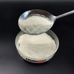
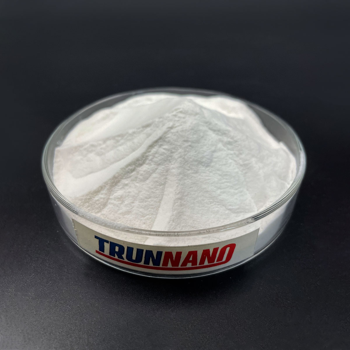
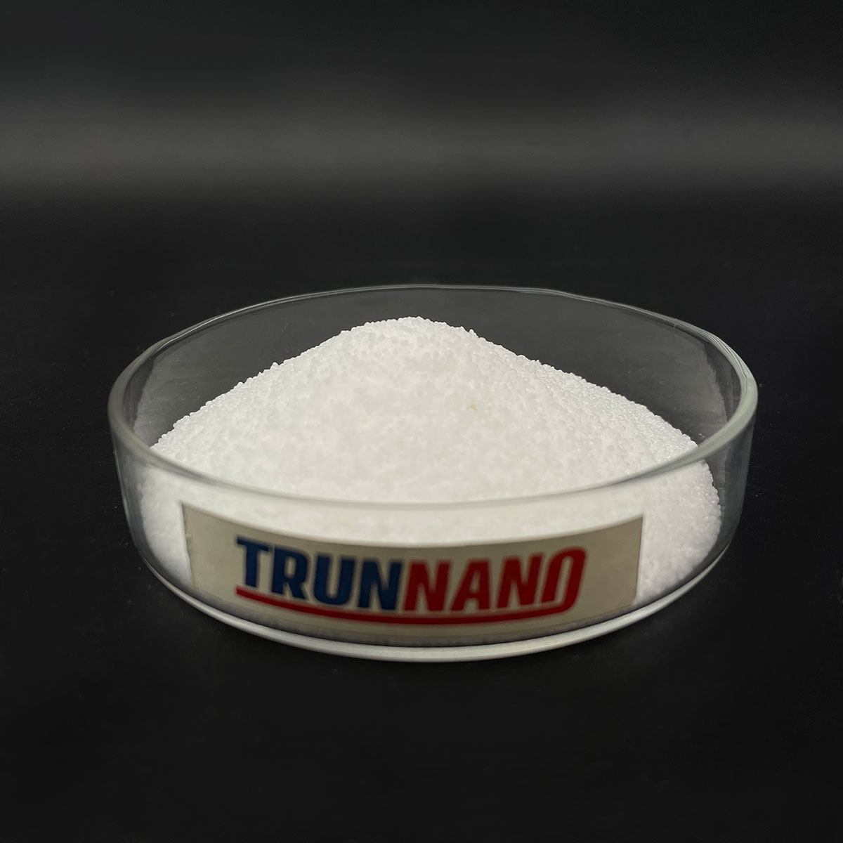
Hexagonal Boron Nitride BN Powderproduced by TRUNNANO is characterized by high purity and stable performance, and is available in a variety of particle sizes. We will provide you with low price and high quality service.