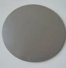
About Metal Alloy 99.95% High Purity Polished Tungsten Wafer:
Tungsten wafer is a material based on tungsten, which has good conductivity and high-temperature stability and is widely used in fields such as microelectronics, semiconductors, and integrated circuits. In microelectronics, tungsten wafers are used as substrate materials for chip manufacturing, providing good conductivity, thermal conductivity, and high thermal stability, which can meet the high-temperature process requirements of chip manufacturing.
Tungsten wafers also play an important role in semiconductor manufacturing processes. When manufacturing semiconductor devices, various materials are required, among which tungsten is one of the most important materials. Tungsten wafers can be used as substrate materials for semiconductor devices, providing good conductivity and thermal conductivity and high thermal stability, which can maintain stable performance in high-temperature processes.
In addition to its microelectronics and semiconductor manufacturing applications, tungsten wafers can also be applied in power electronics. In the field of power electronics, it is necessary to use materials with high conductivity and heat resistance to manufacture power electronic devices, and tungsten wafers precisely meet these requirements. The high conductivity of tungsten wafers can reduce the resistance loss of power electronic devices and improve their efficiency. Its high heat resistance can operate stably in high-temperature environments, ensuring the reliability and stability of power electronic devices.
Complex process steps are required when manufacturing tungsten wafers, including melting, ingot casting, heat treatment, processing, and testing. The manufacturing of tungsten wafers requires the use of high-precision equipment and advanced process technology to ensure high consistency and reliability. Due to the difficulty and high cost of manufacturing tungsten wafers, their prices are relatively high.
However, with the continuous progress of technology and the expansion of application fields, the market demand for tungsten wafers is also increasing.
Due to high conductivity, heat resistance, and high-temperature stability, tungsten wafers have been widely used in fields such as microelectronics, semiconductors, and integrated circuits. With the continuous development of technology, the application prospects of tungsten wafers will also be broader. In the future, with the continuous development of integrated circuits and microelectronics technology, the application fields of tungsten wafers will also continue to expand. For example, in new power semiconductor devices, the high conductivity and heat resistance of tungsten wafers will help improve the performance and reliability of the device. In optoelectronics, tungsten wafers' transparency and high-temperature resistance can be used to manufacture highly reliable optoelectronic devices.
In addition to its applications in microelectronics and semiconductors, tungsten wafers can be applied in other fields. For example, in aerospace, tungsten wafers can manufacture high-performance aerospace components due to their high density and strength. In the medical field, tungsten wafers have good biocompatibility and can be used to manufacture highly reliable medical equipment components.
Properties: low thermal expansion and good thermal conductivity, sufficient resistance to electrical resistance, high elastic modulus.
Applications: widely used in aerospace, electronics, lighting, medical equipment, vacuum coating, electric vacuum stove electrode, heat insulation screen, etc as the radiation shielding material and radiation-protective equipment.
Following is the normal tungsten rod dimension form. For any special dimension, please feel free to contact us and send an enquiry.

Payment & Transportation:

Metal Alloy 99.95% High Purity Polished Tungsten Wafer Properties |
|
| Other Names | Tungsten wafer |
| CAS No. | N/A |
| Compound Formula | W |
| Molecular Weight | N/A |
| Appearance | wafer |
| Melting Point | N/A |
| Solubility in water | N/A |
| Density | N/A |
| Purity | N/A |
| Size | customized |
| Boling point | N/A |
| Specific Heat | N/A |
| Thermal Conductivity | N/A |
| Thermal Expansion | N/A |
| Young's Modulus | N/A |
| Exact Mass | N/A |
| Monoisotopic Mass | N/A |
Metal Alloy 99.95% High Purity Polished Tungsten Wafer Health & Safety Information |
|
| Safety Warning | N/A |
| Hazard Statements | N/A |
| Flashing point | N/A |
| Hazard Codes | N/A |
| Risk Codes | N/A |
| Safety Statements | N/A |
| RTECS Number | N/A |
| Transport Information | N/A |
| WGK Germany | N/A |