
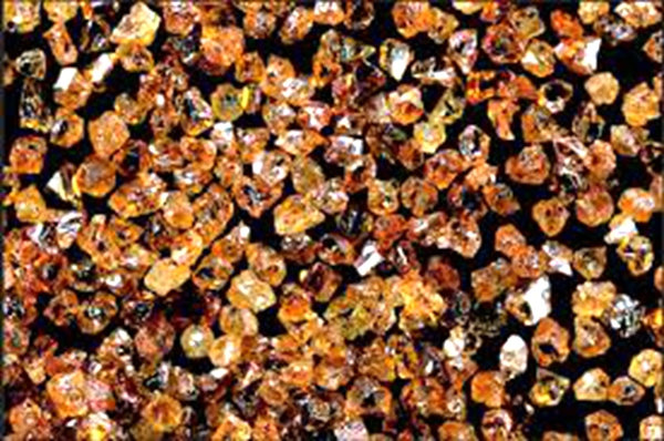
Tiny material with great potential: Boron nitride
Because of excellent thermal and chemical stability, boron nitride ceramics are traditionally used as parts of high –temperature equipment. Boron nitride has potential use in nanotechnology. Nanotubes of BN can be produced that have a structure similar to that of carbon nanotubes, i.e. grapheme (or BN) sheets rolled on themselves, but the properties are very different.
Thermal conductivity. Atomically thin boron nitride has one of the highest thermal conductivity coefficients (751 W/mK at room temperature) among semiconductors and electrical insulators, and its thermal conductivity increases with reduced thickness due to less intra-layer coupling.
Better surface adsorption. Atomically thin boron nitride has been found to have better surface adsorption capabilities than bulk hexagonal boron nitride. According to theoretical and experimental studies, atomically thin boron nitride as an adsorbent experiences conformational changes upon surface adsorption of molecules, increasing adsorption energy and efficiency. The synergic effect of the atomic thickness, high flexibility, stronger surface adsorption capability, electrical insulation, impermeability, high thermal and chemical stability of BN nanosheets can increase the Raman sensitivity by up to two orders, and in the meantime attain long-term stability and extraordinary reusability not achievable by other materials.
Dielectric properties. Atomically thin hexagonal boron nitride is an excellent dielectric substrate for graphene, molybdenum disulphide (MoS2), and many other 2D material-based electronic and photonic devices. As shown by electric force microscopy (EFM) studies, the electric field screening in atomically thin boron nitride shows a weak dependence on thickness, which is in line with the smooth decay of electric field inside few-layer boron nitride revealed by the first-principles calculations.
Raman characteristics. Raman spectroscopy has been a useful tool to study a variety of 2D materials, and the Raman signature of high-quality atomically thin boron nitride was first reported by Gorbachev et al. and Li et al. However, the two reported Raman results of monolayer boron nitride did not agree with each other. Cai et al., therefore, conducted systematic experimental and theoretical studies to reveal the intrinsic Raman spectrum of atomically thin boron nitride. It reveals that atomically thin boron nitride without interaction with a substrate has a G band frequency similar to that of bulk hexagonal boron nitride, but strain induced by the substrate can cause Raman shifts. Nevertheless, the Raman intensity of G band of atomically thin boron nitride can be used to estimate layer thickness and sample quality.

The boron nitride nanomesh is not only stable to decomposition under vacuum, air and some liquids, but also up to temperatures of 800 °C. In addition, it shows the extraordinary ability to trap molecules and metallic clusters which have similar sizes to the nanomesh pores, forming a well-ordered array. These characteristics promise interesting applications of the nanomesh in areas like catalysis, surface functionalisation, spintronics, quantum computing and data storage media like hard drives.
Advancements in Synthesis Technologies
The widespread application of BN nanostructures has long been limited by traditional synthesis methods, which often suffer from low yield, poor purity, high cost, and difficulty in controlling morphology. However, recent breakthroughs have addressed these bottlenecks, paving the way for large-scale industrial production. A notable advancement is the sulfur-catalyzed flash joule heating (FJH) technique reported by researchers from Rice University and other institutions in 2025, which enables the controllable synthesis of BN nanotubes (BNNTs) and nanosheets (BNNSs) in just one minute. This method uses carbon felt as a heating element, achieving a constant temperature of 1200 °C in 30 seconds with a temperature fluctuation of less than 3%, effectively solving the carbon doping problem and achieving a product purity of up to 96.9%.
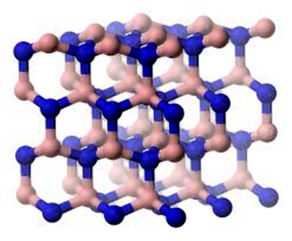
Hexagonal Boron Nitride
By optimizing reaction parameters and adding 5 wt% sulfur as a catalyst, the selectivity of BNNTs can be increased from 19.5% to 60.7%, with a yield of 67.2%, and a high-throughput preparation of 5 grams per batch has been verified, demonstrating great potential for large-scale application. In addition, advancements in chemical vapor deposition (CVD) techniques have further improved the quality and scalability of BN materials. For example, pyrolytic boron nitride (PBN) synthesized via CVD exhibits high density and purity, making it ideal for high-temperature components in electronics and aerospace. Template-assisted CVD and precursor pyrolysis methods have also been refined to produce continuous BN fibers and large-area monolayer BN films, which are crucial for applications in composite materials and 2D electronics.
Surface modification is another key area of progress in BN synthesis. Recent studies have shown that modifying nanosized BN with carboxylic acids of different chain lengths (such as succinic acid, adipic acid, and sebacic acid) can significantly improve its compatibility with polymer matrices. This modification reduces the viscosity of BN-polymer composites, enhances their adhesion to metal substrates (such as silver, copper, and gold), and maintains excellent thermal conductivity, expanding the application of BN in high-power electronics and adhesive materials.
Cutting-Edge Applications in Emerging Fields
The unique combination of properties of BN materials has driven their rapid penetration into emerging high-tech fields. In the electronics industry, BN has become a critical material for thermal management and dielectric substrates. With the increasing power density of advanced microelectronics, traditional printed circuit board (PCB) substrates can no longer meet the thermomechanical and dielectric requirements. A recent study has developed a borosilicate glass-hexagonal BN (h-BN) nanocomposite for PCB substrates, which exhibits a 3-fold increase in fracture toughness, a 13% increase in elastic stiffness, and a 100% improvement in DC dielectric breakdown strength compared to pristine glass. This composite also reduces the dielectric constant, mitigating signal propagation latency and capacitive coupling, making it ideal for next-generation wide-bandgap power electronics and high-frequency packaging
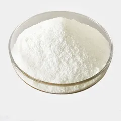
Technical Parameter of Boron Nitride BN powder:
|
Product Name |
MF |
Purity |
Particle Size |
Melting Point |
Density |
Color |
|
boron nitride |
BN |
99% |
100nm, 500nm, 3-5um,10-20um, 20-50um,50-100um |
3000℃ |
2.29 |
white |
Chemical Composition of Boron Nitride BN powder:
|
BN |
MgO |
Na2O |
Fe2O3 |
CuO |
MnO |
|
99% |
0.068% |
0.08% |
0.06% |
0.012% |
0.0253% |
In the energy storage field, twist angle engineering has opened up new possibilities for BN applications in sodium-ion batteries (SIBs). Density functional theory studies show that adjusting the stacking configuration and twist angle of BN can significantly enhance its electrochemical properties. For example, the ab-BN-21.8° twisted structure retains excellent mechanical properties while reducing the Na⁺ interlayer diffusion barrier and interlayer expansion, and Na insertion significantly improves its electronic conductivity. This makes twisted BN a promising anode material for high-performance SIBs, providing theoretical guidance for the design of next-generation 2D energy storage materials.
In aerospace and nuclear energy, BN materials play an indispensable role in protecting against extreme environments. Their high thermal stability and radiation resistance make them ideal for shielding rocket engines from ultra-high temperatures (exceeding thousands of degrees Celsius) and for detecting nuclear radiation. BN-based composites are also used in high-temperature structural components, where their lightweight and high-strength properties help reduce the weight of aerospace vehicles while ensuring structural integrity.
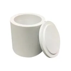
Boron Nitride Crucible
Challenges and Future Outlook
Despite the remarkable progress in BN research and application, several challenges remain to be addressed. First, the large-scale synthesis of high-quality BN nanostructures (especially monolayer BN films and BNNTs) still requires further optimization to reduce costs and improve yield. Although the FJH technique has achieved high-throughput synthesis, its industrialization still faces technical hurdles such as equipment scaling and process stability. Second, the integration of BN materials with other functional materials (such as 2D semiconductors and polymers) needs to be improved to enhance interfacial compatibility and realize synergistic performance. Third, the fundamental understanding of the structure-property relationship of BN, especially the influence of stacking configuration, twist angle, and surface defects on its properties, is still incomplete, which limits the precise design of BN-based materials for specific applications.
Looking ahead, the future of BN materials lies in the integration of advanced synthesis technologies, property engineering, and multidisciplinary applications. With the deepening of twist angle engineering, surface modification, and dimension control, it is expected to develop BN materials with tailored properties for specific scenarios, such as high-efficiency energy storage, ultra-high-temperature protection, and high-sensitivity sensing. The combination of BN with other 2D materials (such as graphene and MoS2) will also open up new possibilities for next-generation nanoelectronics and optoelectronics. In addition, the industrialization of low-cost, high-purity BN synthesis techniques will promote its widespread application in traditional industries and emerging fields, making this tiny material a key driver of technological innovation in the 21st century.
Composites containing BN
Addition of boron nitride to silicon nitride ceramics improves the thermal shock resistance of the resulting material. For the same purpose, BN is added also to silicon nitride-alumina and titanium nitride-alumina ceramics. Other materials being reinforced with BN include alumina and zirconia, borosilicate glasses, glass ceramics, enamels, and composite ceramics with titanium boride-boron nitride, titanium boride-aluminium nitride-boron nitride, and silicon carbide-boron nitride composition.
Supplier
TRUNNANO (Luoyang Trunnano Tech Co., Ltd ) is a professional boron nitride manufacturer with over 12 years experience in chemical products research and development. If you are looking for high quality boron nitride, please feel free to contact us and send an inquiry.